Silicon Photonics
Silicon photonics has the potential to radically change the landscape of photonics. Its compatibility with well-known and mature CMOS fabrication technology offers advantages, such as low-cost, high-volume and reliable manufacturing with nanoscale precision. Applications can typically be found in telecommunication and data-communication, sensing and advanced instrumentation. Integration with CMOS-based electronics allows for adding the driver and control electronics on the same chip, greatly reducing packaging complexity and cost. Vice-versa the addition of a photonic layer and interconnects hold the promise of solving speed bottlenecks in future computing and chip platforms.
Breakthroughs in silicon photonics have been achieved with high-speed silicon modulators, nanophotonic components such as ring resonators and filters, and photodetectors based on silicon-germanium alloys, which can operate in the range of the important telecommunication wavelengths of 1.3 μm and 1.55 μm. However because of its indirect bandgap optical amplifiers and sources, such as lasers, are difficult to realize in silicon.
[Our group] has developed a unique approach to create active optical components on silicon where the light that is confined in the silicon waveguide couples evanescently to an optically active layer bonded on top of it. This layer is composed of III/V semiconducting materials, such as indiumphosphide-based alloys, which are the traditional materials of choice for high-performance photonic applications. In this approach the silicon photonic components can be patterned first in a CMOS compatible process. Bonding of the III/V material does not require precise alignment and the consequent III/V processing does not affect the silicon components. On this platform we have successfully realized lasers operating at wavelengths of 1.3 μm and 1.55 μm, optical amplifiers, detectors and modulators. Our current goal is to increase integration density on this hybrid silicon platform by combining different components on the same chip to create increased functionality, speed and capacity. To this end we also aim to minimize the footprint of the components by reducing their size, for example using micro-ring lasers.
Lasers
Heterogeneous integration by direct wafer bonding of a III-V active region to pre-patterned silicon-on-insulator (SOI) waveguides has been successfully demonstrated as a promising technology to address the challenge of realizing an efficient transfer on silicon. This technique utilizes III-V material for optical gain/modulation and silicon for optical wave-guiding and does not require any alignment during bonding. Using taper structures, the evanescent optical mode between the III-V and silicon can be completely transferred to the SOI waveguide, enabling integration with other silicon based optical devices. Using this approach, a variety of discrete active devices such as distributed feedback (DFB), distributed Bragg reflector (DBR), ring, fabry-perot and AWG lasers have been fabricated.
Modulators
Silicon photonics is of interest because it uses the same substrate as and process techniques compatible with modern CMOS fabrication. For high speed applications, one of the hurdles is the lack of efficient modulators for the bit rate above 40 Gb/s. Most of the modulators reported on silicon substrate suffer from the tradeoff among the bandwidth, modulation efficiency and the insertion loss due to the limitation mainly from the material systems.
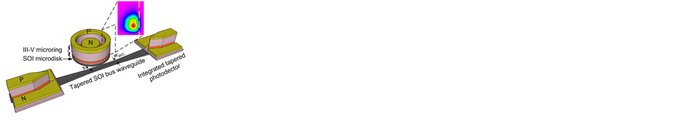
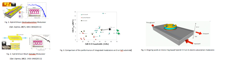
We are developing the modulators based on our hybrid silicon platform, where the III-V material bonded on the SOI wafer can achieve excellent optical modulation originating from the strong electroabsorption effect and electrorefractive effect. The prototype devices we have developed have shown record performance on speed (Fig. 1) and extinction ratio (Fig. 2) in this field. Fig. 3 shows the comparison of the performance for the integrated modulators on silicon or indium phosphide substrate. It also points out the target of the next generation that we are now working for. Fig. 4 shows the schematic of a hybrid III-V on Si modulator design using a micro-ring resonator. Micro-ring structures inherently have a small footprint and hence lower cost.
PICs
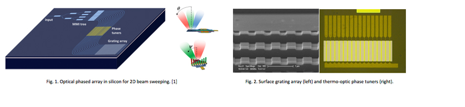
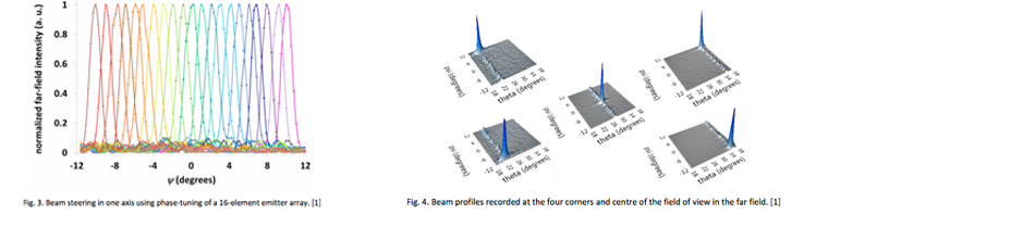
Optical phased arrays allow free-space beam steering without the need for mechanical operation, which is of interest for robust point-to-point free-space communications, Light Detection and Ranging (LIDAR), and optical memory. Realizing such devices in a manner compatible with standard CMOS fabrication is advantageous in that it allows them to be fabricated alongside the electronics used to drive them, thus lowering cost, reducing packaging complexity, and minimizing size. We are developing a beam steerer based on the hybrid silicon platform such that optical sources, gain elements, phase modulators, surface gratings, waveguides, and detectors can be integrated together on standard silicon-on-insulator. The devices demonstrated thus far have employed thermo-optic phase modulation and waveguide surface grating arrays to achieve two-dimensional far field beam steering over a 20⁰ x 14⁰ field of view with 10 dB background suppression and 0.6⁰ x 1.6⁰ beam width. This research was supported by the DARPA Sweeper program, grant #HR0011-10-2-0003.
Photodetectors
Our group photodetector research is focused on individual photodiodes for coherent and analog applications as well as integration technologies for photonic integrated circuits with greater levels of complexity. Silicon is an excellent material for optoelectronic receivers (and other photonic circuits) due to its low material loss, but a poor absorber of infrared light for the same reason. Germanium is an attractive absorbing material for silicon photonics because it can be grown directly on silicon substrates and then processed in a CMOS fab. Our group is currently working on novel designs for germanium on silicon photodetectors for analog and coherent communications. The high thermal conductivity of silicon should give these detectors an advantage over traditional III-V detectors in these high-power receiver applications.

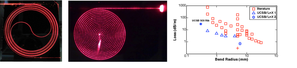
Ultra-low-loss Waveguides
Planar waveguides with ultra-low propagation loss are necessary for the long propagation distances and high quality factor resonators used in photonic rotational velocity sensors, true-time-delay networks, optical buffers, and narrowband photonic filters. In most silica-based planar waveguide platforms, the optical mode is highly confined to a low-index-contrast core that is several microns in width and height. With core confinement factors greater than 70% calculated for an index contrast of 0.7% and a free-space wavelength of 1550 nm, the quality of the core material is emphasized in these structures. Since the cladding material is typically SiO2, the small refractive index contrast is created through the deposition of doped SiO2 cores.
In a recent collaboration with LioniX BV, we demonstrated record low 0.7 dB/m single-mode propagation loss for the TE mode in planar silica-on-silicon spiral waveguide delays having a fixed index contrast of ~23%. Due to the thin core geometry in these structures, the core confinement factor is about 3%, and a majority of the optical mode propagates in the undoped silicon dioxide cladding layers. The large effective mode area that results from the high-aspect-ratio core geometry of our waveguides, calculated to be around 5 μm2 at a free-space wavelength of 1550 nm, and a photoresist reflow process contribute to the reduction of interfacial scattering loss. Additional photonic components, including ultra-high-Q ring resonators, multi-mode interferometers, polarizers, Mach-Zehnder interferometers, and arrayed-waveguide gratings have been demonstrated with this planar waveguide platform.