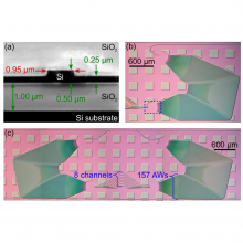
Low-loss arrayed waveguide gratings (AWGs) are demonstrated at a 2.0-μm wavelength. These devices promote rapidly developing photonic applications, supported by the recent development of mid-infrared lasers integrated on silicon (Si). Multi-spectral photonic integrated circuits at 2.0-μm are envisioned since the AWGs are fabricated with the 500-nm-thick Si-on-insulator platform compatible with recently demonstrated lasers and semiconductor optical amplifiers on Si. Characterization with the AWG- ring method improves the on-chip transmission uncertainty to ∼6% compared to the conventional method with an uncertainty of ∼53%. Channel losses of ∼2.4 dB are found, with −31 dB crosstalk per channel. Fully integrated multi-spectral sources at 2.0 μm with pump lasers, low-loss multi-plexers, and an output amplifier are now feasible.