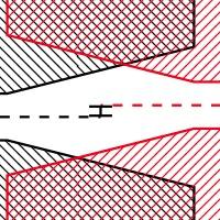
While Moore’s law predicted shrinking transistors would enable exponential scaling of electronic circuits, the footprint of photonic components is limited by the wavelength of light. Thus, future high-complexity photonic integrated circuits (PICs) such as petabit-per-second transceivers, thousand-channel switches, and photonic quantum computers will require more area than a single reticle provides. In our novel approach, we overlay and widen waveguides in adjacent reticles to stitch a smooth transition between misaligned exposures. In SiN waveguides, we measure ultralow loss of 0.0004 dB per stitch, and produce a stitched delay line 23 m in length. We extend the design to silicon channel waveguides, and predict 50-fold lower loss or 50-fold smaller footprint versus a multimode-waveguide-based method. Our approach enables large-scale PICs to scale seamlessly beyond the single-reticle limit.