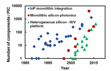
Heterogeneous silicon photonics using wafer bonding is reaching maturity with commercial products for the data center market being shipped in volume. Here we give an overview of recent research in the area showing record device performance by using the best of both worlds: III-V for light generation and Si for guiding the light. Utilizing the flexibility of the heterogeneous silicon platform, narrow-linewidth widely tunable lasers as well as fully integrated mode locked lasers with record pulse powers and pulse duration were demonstrated. The ability to perform multiple die bonding with optimized epitaxially grown layer stacks was used to realize high-performance photonic integrated circuits both for communications and sensing. In addition to III-V materials, nonreciprocal materials such as, for example, Ce:YIG can be bonded, providing additional functionality such as on-chip isolators and reconfigurable on-chip circulators. On-chip isolation will become necessary with the increase in complexity of photonic integrated chips as photonic components such as lasers are sensitive to feedback effects.