Email
Position
Engineer
Department
Electrical and Computer Engineering
Office Location
ESB 2221G
Biography
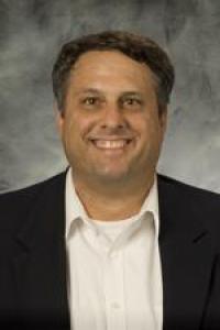
Jon has over 13 years of process experience in the MEMS and semiconductor field. He worked at Applied Magnetics Corporation in Santa Barbara as an operator, process inspector, and plate & etch technician for five years before moving to Solus Micro Technologies/NP Photonics in Westlake Village as a Process Engineer for four years. Jon moved back to Santa Barbara to work at Innovative Micro Technology as a Process Engineer and R & D Engineer for four years before coming to work for the Bowers group at UCSB in 2008.