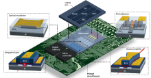
Artificial intelligence, machine learning and high-performance computing workloads are pushing electrical input/output to its limits in signal reach, energy efficiency and bandwidth density, turning optics from option to necessity. Complementary metal–oxide– semiconductor-integrated silicon photonics offers a practical path forward by combining high-volume manufacturing with mature photonic building blocks. This Review presents progress across devices (on-chip lasers and semiconductor optical amplifiers, compact modulators, high-speed photodetectors, low-loss routing and efficient chip–fibre couplers), multimaterial integration (hybrid assembly, heterogeneous wafer bonding, microtransfer printing and monolithic epitaxy) and electronics co-design (digital signal processing, serializer/deserializer, stacked-driver topologies, bias control and thermal tuning) to show how total link energy is being driven towards the sub-picojoule per bit regime. We connect these advances to system architectures that are evolving from pluggables to linear-drive pluggables and co-packaged optics, and we discuss the trade-offs among bandwidth density, thermal design, yield and cost. We identify near-term bottlenecks, notably thermal pathways and manufacturing yield, and highlight technologies most likely to unlock the next jump in performance, including on-chip comb sources for dense wavelength-division multiplexing and wafer-scale 3D electronic and photonic stacks. The same platform is poised to impact optical compute input/output, sensing and quantum photonics, linking device-level innovation to system-level gains across computing and communications.
Please check out the full article below.
