Events & Seminars
| Dissertation Defense | November 29, 2023, 10:00 am | Eamonn Hughes | Characterizing and Controlling the Impact of Dislocations on the Reliability of InAs Quantum Dot Lasers
Dissertation Defense Eamonn Hughes WEDNESDAT, November 29th AT 10:00AM ZOOM MEETING - Click Here to Join
… |
||
| Monolithic mode-locked semiconductor frequency comb laser pulse generation and stabilization | January 31, 2020, 10:00 am | 
|
Dominik Auth, Stefan Breuer, John A. Paulson | Institute of Applied Physics, Technische Universität Darmstadt, Darmstadt, Germany & School of Engineering and Applied Sciences, Harvard University, Cambridge, USA | We review advances in the timing stabilization of self mode-locked and passively mode-locked |
| Nanoscale Foundries: Electronics, Photonics, Ionics, Fluidics | January 28, 2020, 12:00 am | 
|
Dr. Rajeev Ram | Department of Electrical Engineering & Computer Science, MIT | Nanoscale Foundries: Electronics, Photonics, Ionics, Fluidics Dr. Rajeev Ram Department of Electrical Engineering & Computer Science, MIT
Modern silicon fabs routinely produce functional electrical components for a few dollars at part counts exceeding billions per year and a complexity rivaling the human genome. The productivity of these fabs is ensured by design rules that govern the structures that constitute these systems. These… |
| Electronic-Photonic Co-Design; from Energy Efficient Imaging to Optical Phase Control | May 23, 2019, 4:00 pm | 
|
Firooz Aflatouni | Skirkanich Assistant Professor, Department of Electrical and Systems Engineering, University of Pennsylvania | Abstract: Integrated electronic-photonic co-design can profoundly impact both fields resulting in advances in several areas such as energy efficient communication, signal processing, imaging, and sensing. Examples of integrated electronic-photonic co-design may be categorized into two groups: (a) electronic assisted photonics, where integrated analog, RF, mm-wave, and THz circuits are employed to improve the performance of photonic systems, and (b) photonic assisted electronics, where… |
| The butterfly effect in quantum cascade lasers: Why and What? | February 28, 2019, 4:00 pm | 
|
Frédéric Grillot | Professor, Télécom ParisTech | ABSTRACT: The quantum cascade (QC) laser is a promising light source based on resonant tunneling and optical intersubband transitions between quantized conduction band states. In these semiconductor lasers, the principles of operation arise from the quantum engineering of electronic energy levels and tailoring of their wavefunctions [1]. The opportunity given by the broad span of wavelengths that QC lasers can achieve, from mid-infrared to terahertz, leads to a wide number… |
| Integrated-Photonics Frequency Combs: Precision Metrology, Optical Synthesis, and Nonlinear Optics on the Nano-Scale | January 25, 2019, 10:00 am | 
|
Tara Drake | NRC postdoc fellow, National Institute of Standards and Technology | The invention of optical-frequency combs has transformed the fields of precision metrology, spectroscopy, and electronic/photonic signal generation. Now, a new and incredibly promising platform for frequency combs has emerged—one in which phase coherent combs are generated in nanofabricated ring resonators using quantum nonlinear photonics. I will present our work designing the first octave-… |
| Integrated Nanophotonic Technologies for Quantum Information Science | January 23, 2019, 10:00 am | 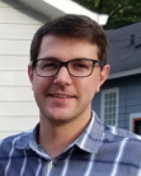
|
Galan Moody | Research Scientist, National Institute of Standards and Technology (NIST) | Abstract: Quantum information science (QIS) technologies for computing, communications, sensing, and metrology rely on the ability to generate and detect non-classical information using light and matter. Photonics plays a central role in QIS because of the inherent scalability and low-loss, high-speed transmission of light. Yet, despite its ubiquitous presence, there are no high-… |
| Monolithic integration of III/V-based functionalities to CMOS-based Si-micro- and nanoelectronics | December 8, 2017, 9:00 am | 
|
Wolfgang Stolz | Professor, Philipps-Universität Marburg; Co-Founder of NAsP III/V GmbH | Abstract: In recent years, the monolithic integration of III/V-semiconductor materials and heterostructures on CMOS-compatible (001) Si-substrate is gaining increasing interest for the realization of novel integrated circuits with improved electronic, optoelectronic or photonic functionalities. The principal challenges of the III/V-material integration on CMOS-compatible (001) Si-substrates will be reviewed and possible solutions for the high-quality… |
| Semiconductor quantum dot lasers: Why are they so quantum? | November 20, 2017, 2:00 pm | 
|
Frédéric Grillot | Professor, Télécom ParisTech, France, Research Professor, University of New-Mexico, USA | Abstract: By the reduction of semiconductor structure dimensionality, from bulk to quantum-well and finally to quantum-dots (QDs), we gain in control over the energetic distribution of carriers and their interaction with light [1]. While in bulk material many electron states, which are distributed in energy and momentum, have to be occupied, only a few states near the bandgap can contribute to the optical gain in lasers. Over the last past years, tremendous efforts have been… |
| Advances in Energy Efficiency through cloud and ML | October 20, 2017, 4:30 pm | 
|
Urs Hölzle | Senior Vice President, Technical Infrastructure & Google Fellow | Abstract: Today, the IT industry accounts for about 2 percent of total greenhouse gas emissions, comparable to the footprint of air travel. This footprint includes everything from datacenters and servers to networks and client equipment like laptops and printers. More and more information is being generated every day, and more and more consumers and enterprises are processing this information every day. Will IT emissions eclipse air travel one day soon? |
| 2D material-based layer transfer based on remote epitaxy & uniform epitaxial RAM towards large-scale neuromorphic arrays | July 14, 2017, 10:00 am | 
|
Jeehwan Kim | Massachusetts Institute of Technology | Bio: Professor Jeehwan Kim joined the Mechanical Engineering faculty at Massachusetts Institute of |
| Semiconductor Nanowires for Optoelectronic and Energy Applications | June 9, 2017, 12:00 pm | 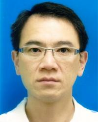
|
H. Hoe Tan | Head of the Department of Electronic Materials Engineering at the Research School of Physics and Engineering, The Australian National University | Bio: Professor H. Hoe Tan is currently the Head of the Department of Electronic Materials Engineering at the Research School of Physics and Engineering, The Australian National University. He received his B.E. (Hons) in Electrical Engineering from the University of Melbourne in 1992, after which he worked with Osram in Malaysia as a quality assurance engineer. In 1997, he was awarded the PhD degree from the Australian National University for his dissertation on "Ion beam… |
| High-Resolution Quantitative Cathodoluminescence (CL) for Defect Metrology in Semiconductors | April 7, 2017, 8:30 am | 
|
Samuel Sonderegger | CEO & Co-Founder of Attolight AG | Abstract: High spatial resolution spectroscopic information may be acquired by using an electron beam in a modern scanning electron microscope (SEM), exploiting a phenomenon called cathodoluminescence (CL). CL can be used to perform non-destructive analysis of a broad range of materials comprising insulators, semiconductors and metals. This approach offers several advantages over usual optical spectroscopy techniques. The multimode imaging capabilities of the SEM enable the… |
| More-than-Moore with Integrated Silicon-Photonics | March 30, 2017, 4:00 pm | 
|
Vladimir Stojanovic | Associate Professor, Electrical Engineering & Computer Science, UC Berkeley | Abstract: In this talk we'll present the latest results on the integration of silicon-photonic interconnects into a monolithic platform (45nm SOI logic process and bulk CMOS memory periphery process). These include world's first microprocessor communicating to the outside world with monolithically integrated Si-Photonic devices, as well as the first demonstration of photonics in a bulk CMOS process. We’ll also illustrate some critical aspects of this technology that need to… |
| Nonlinear Optics in AlGaAs: Past, Present and Future Prospects | March 13, 2017, 12:00 pm | 
|
J. Stewart Aitchison | University of Toronto, Department of Electrical and Computer Engineering | Abstract: The III‐V semiconductor AlGaAs is an ideal nonlinear optical material. It has large second and third order nonlinearities, a low two‐photon absorption coefficient at the half band gap and allows for the easy fabrication of integrated optical devices. In additoon, AlGaAs can be used directly integrate photodiodes, modulators and passive optical elements on the same chip as the nonlinear elements. This talk will highlight the benefits of this nonlinear material… |
| Nano Research at the University of Duisburg-Essen: An Overview | March 1, 2017, 4:00 pm | 
|
Tobias Teckentrup | Managing Director, Center for Nanointegration Duisburg-Essen (CENIDE) | Abstract: The Center for Nanoinetgration Duisburg-Essen (CENIDE) is a research center that focuses on nanoscience as the main research area of the University of Duisburg-Essen (UDE, Germany). Since 2005, CENIDE links the activities in natural science, engineering and medicine at the UDE that deal with the nano dimension. The experience of more than 65 working groups is divided into five research areas: Dynamic Processes in Solids, Gas-phase Synthesis, Magnetism,… |
| Compliant III-V On (001) Si Substrates for Direct Laser Growth | January 5, 2017, 4:00 pm | 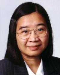
|
Kei May Lau | Fang Professor of Engineering and Chair Professor, Hong Kong University of Science and Technology (HKUST) | Abstract: Integrating high-performance III-V devices on the mature silicon platform has been a long pursuit over the past few decades. Direct epitaxial growth offers an alternative technology to bonding. Using nano-patterned Si substrates, we created III-V on silicon templates with low defect density and smooth surface morphology for laser growth. Such antiphase-domain (APD)-free III-V on silicon compliant templates with high crystalline quality (benchmarked by narrow XRD… |
| Optofluidic Integration of Hollow-Core Waveguides for Chip-based Biomolecule Analysis | December 15, 2016, 4:00 pm | 
|
Holger Schmidt | Narinder Singh Kapany Chair of Optoelectronics and Associate Dean for Research for the School of Engineering at UC Santa Cruz | Abstract: Integrated photonic devices have traditionally been designed for data communications using exclusively solid-state materials. However, a vast area of potential applications, in particular in the life sciences, involve interactions of light with liquids and gases. Recently, a number of optofluidic approaches have been considered that are aimed at integrating such non-solid media with chip-scale photonic structures. We have developed a versatile, planar photonic… |